Lithopane Lightbox
A Bluetooth-controlled multi-color lightbox that illuminates a 3D lithopane to display an image
Controller PCB
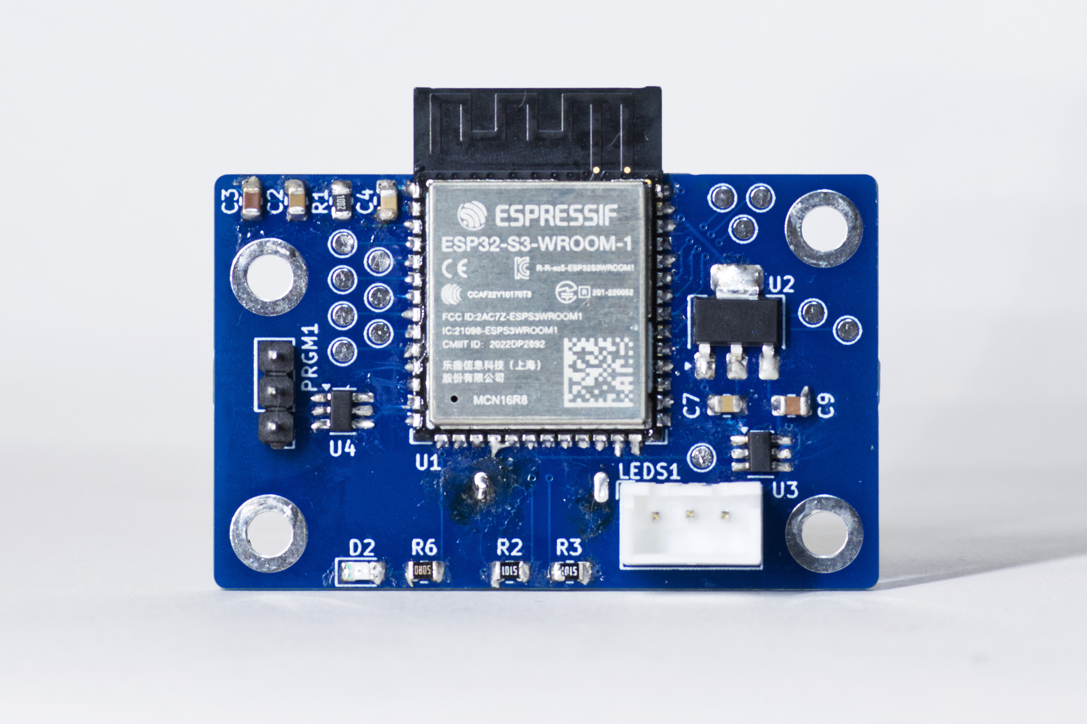
I designed this PCB around an ESP32-S3 SoC. It runs the NimBLE Bluetooth Low-Energy (BLE) stack, responding to on/off events and configuration updates sent from a mobile phone. It advertises itself using the GAP protocol and can be paired to a phone. Then, it listens for GATT events and drives the LEDs (on another board) accordingly.
I used an RTOS to manage the BLE stack concurrently with driving the LEDs. Responding to GATT events, BLE state management, and button input all happens reliably. Message queues pass commands and data between tasks.
The ESP32-S3 features a native USB peripheral, so I exposed two GPIOs to a 3-pin header (GND, D+, and D-) labeled PGRM1. I use this header to program and debug the board, and I power the board through its USB-C connector. When mounted in its case, only the USB-C connector, along with a button, are exposed.
The front of the controller PCB
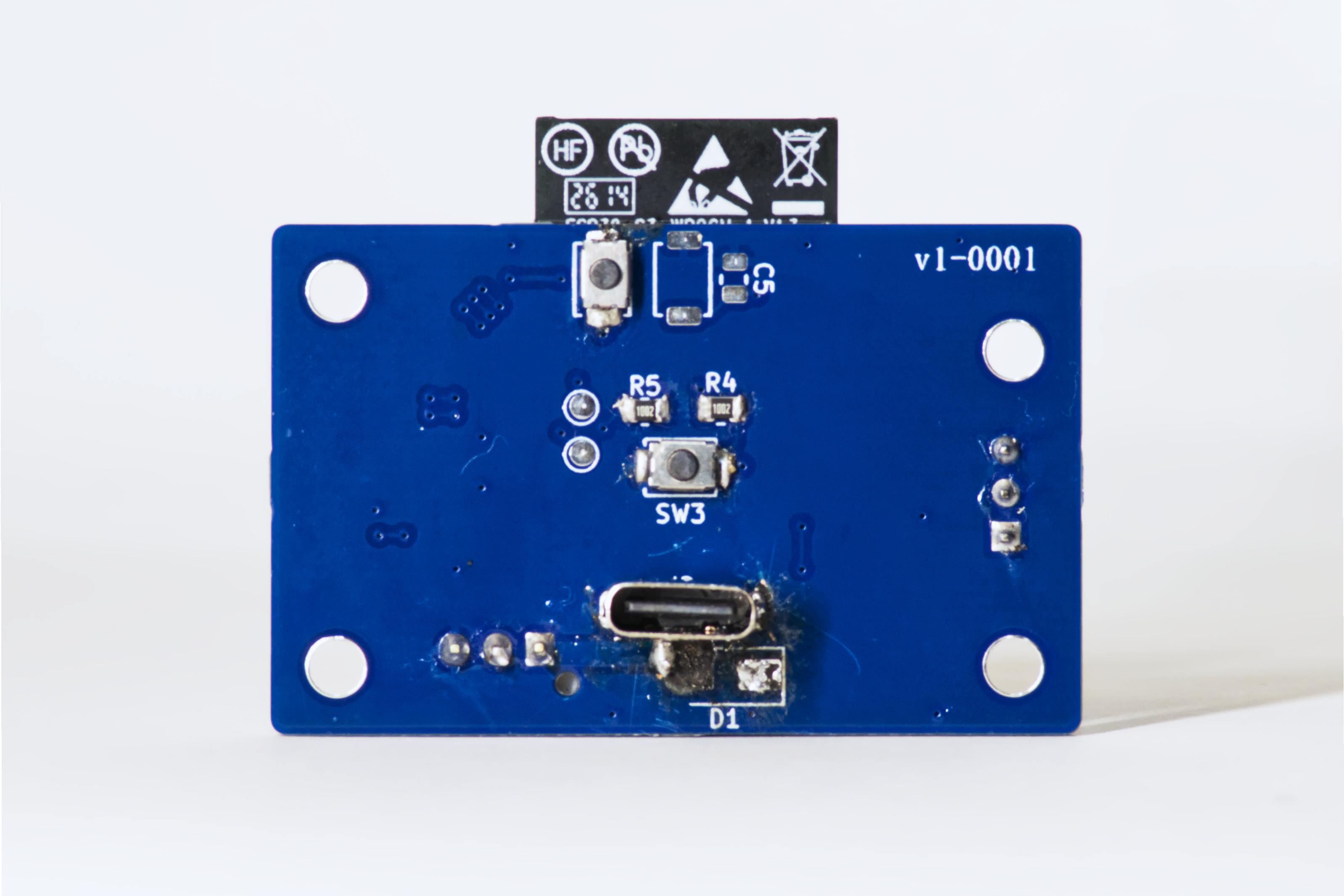
The back of the controller PCB
LED Grid
This PCB holds 54 individually-addressable LEDs of the WS2812B chipset. It is receives power and data input from the controller PCB (above), and adds a bulk capacitor. This stabilizes the voltage across flashing LED patterns, and prevents the ICs inside of each LED from browning out and corrupting the daisy-chained data signal.
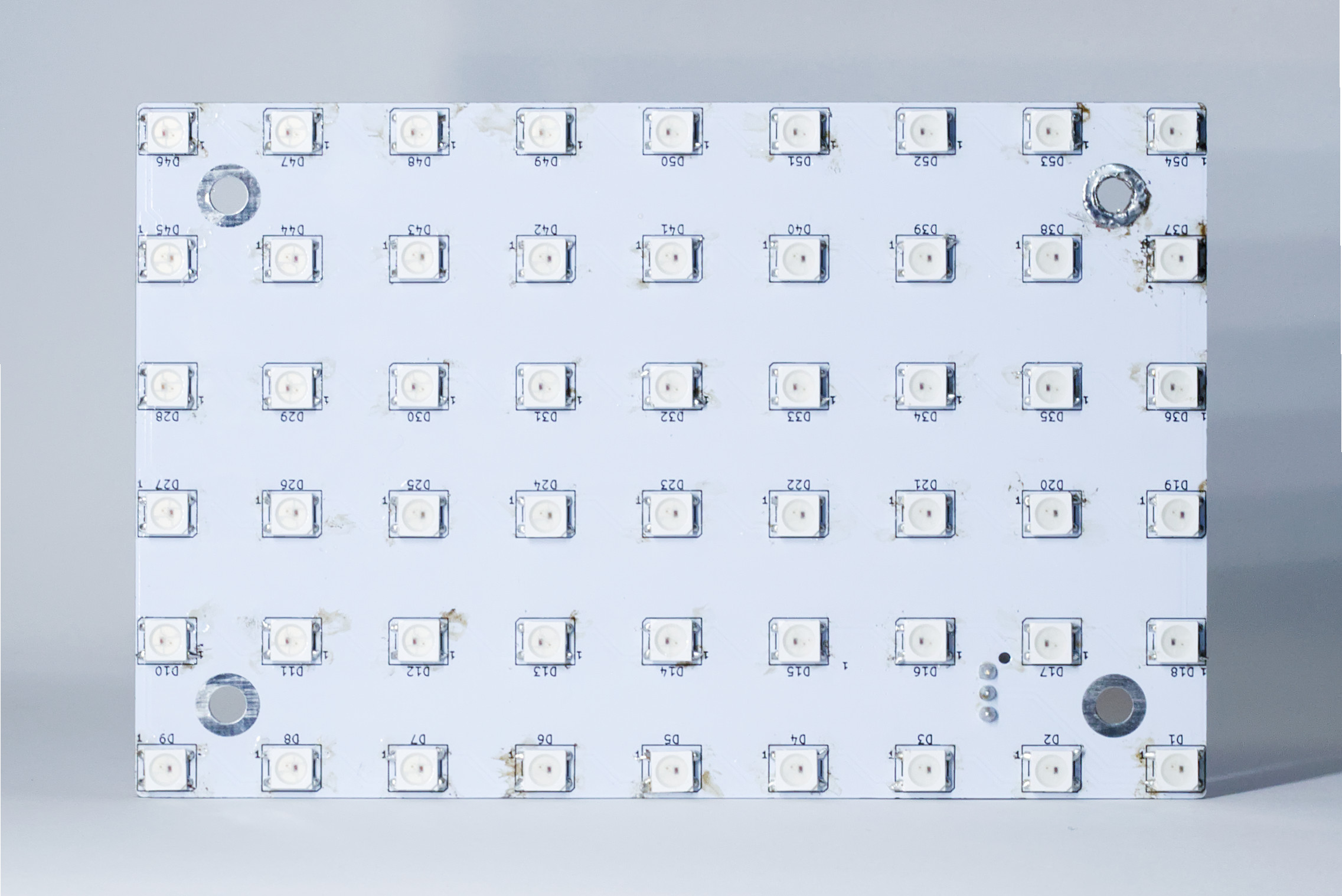
A 9x6 grid of individually-addressable LEDs
Rather than route power traces, the front surface has a 5V plane which the LEDs connect to. This "star"-like configuration minimizes voltage drop and ensures each LED has the same voltage to reference the data signal to, ensuring reliable data transfer. This specific LEDs have internal capacitors, so no external decoupling capacitors are needed.
The back layer has a ground plane. The data signals are chained between LEDs on the front surface so that their return paths have an uninterrupted ground plane to flow through.
© 2026 Rishi Roy
Unless otherwise stated, all images are my own work. (I'm a photographer, after all!)